

Our system has noticed that you are based in , but the current country setting is . Select country
Press Photos
Please note our terms of use governing the use of press images.By downloading the images from our media database, you agree to these terms of use: Press images may only be used for press purposes (print, electronic media, online) and exclusively in the context of the associated press release and may not be edited. The picture credits (source: Wacker Chemie AG) are mandatory. Images deleted from the media database may no longer be used in the future. If a press photo is used, a copy of the publication or a link to the publication is requested. Otherwise, the copyright information www.wacker.com/disclaimer applies.

Lab test - VINNAPAS® EF 8860
Determination of adhesion via peel test: Adhesives formulated with VINNAPAS® EF 8860 are particularly rugged and long-lasting. This makes the new product an ideal dispersion base for flooring adhesives for flexible floor coverings such, especially for PVC floorings.
(JPG, 33 KB) Download picture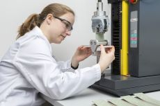

WACKER’s PULPSIL® 968 S
The rate at which pulp slurry is dewatered can be measured in drainage tests. WACKER’s new silicone tensid PULPSIL® 968 S accelerates dewatering to unprecedented levels and improves the washing process during pulp making significantly.
(JPG, 37 KB) Download picture

Polyvinyl acetate solid resins
Polyvinyl acetate solid resins are an essential component of modern, high-quality gumbase. WACKER produces them in compliance with strict quality and hygiene standards.
(JPG, 32 KB) Download picture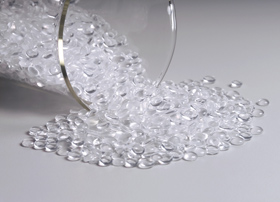

Siltronic - Silicon Ingot
WACKER subsidiary Siltronic produces hyperpure silicon wafers for semiconductor and microelectronics applications. The wafers are sliced off perfect, highly pure monocrystals – so-called hyperpure silicon ingots – that have diameters of up to 300 millimeters.
(JPG, 22 KB) Download picture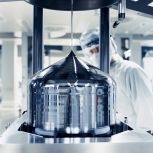

Silicone Adhesive Sealant ELASTOSIL®
In the production of electronic controllers and sensors, ELASTOSIL® silicones seal housing components, bond individual elements and encapsulate electronic parts. Specialty ELASTOSIL® grades are particularly stable to automotive fuels and oils.
(JPG, 33 KB) Download picture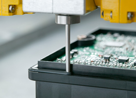