
Surfing by Daylight
Bright ambient light often renders liquid crystal displays hard to read. The main reason for this is a gap between the display and the touch panel. Using a new silicone gel from WACKER and a special production technology called optical bonding, German display-enhancement company VIA optronics makes displays fit for use in bright surroundings.


Standard displays can also be difficult to read in very brightly lit rooms.
Notebook computer displays and touchscreens that have a brilliant, high-contrast image indoors are often hard to read and use outdoors. The colors look faded and lack sharp contrast. Sunlight falling directly onto a display generates dazzling reflections, and the eye only distinguishes a fuzzy patch of light. And it’s the same in very brightly lit rooms.
Displays that are difficult to read in daylight affect not only those using notebooks, flat screen monitors, tablets and smartphones, but also motorists, when navigation systems or the console display lose contrast in bright sunlight.
Virtually all flat-screen displays are affected by these bothersome reflections, including the active-matrix LCDs that currently dominate the market for flat screens. The German Flat-Screen Display Forum (DFF) claims that active-matrix LCDs account for around 90 percent of its sales. “Active-matrix LCDs which operate in transmissive mode offer outstanding color accuracy, which is why they are so popular at the moment,” explains Dr. Karlheinz Blankenbach, chair of the DFF and a professor at Pforzheim University.
Cell acts as light valve

With and without silicone: Schematic drawing of a liquid crystal display; right: conventional design; left: design optically bonded with a specialty silicone gel from WACKER.
Generally, a liquid crystal display does not produce its own light. Its core component, the LCD cell, acts merely as a light valve and requires a light source to produce a visible image. In a transmissive type of LCD, this light is provided by backlighting the LCD cell. “Light-transmissive areas in the LCD cell transmit light and so appear bright. Opaque areas, in contrast, block the light, and are responsible for dark areas,” explains Blankenbach.
When ambient light strikes a display, the screen contents look brightened because our eyes additionally perceive the light reflected from the display. As a result, black areas of the display appear gray in incident light, with the shade of gray becoming progressively lighter with increasing intensity of the incident light. The light-dark contrast is consequently worsened.
“Outdoors, especially, reflections can have such a high luminance that they completely outshine the screen contents and lower the contrast ratio – the ratio of the luminance of the brightest screen area to that of the darkest screen areas – to less than 3:1. At that stage, it’s impossible to read the display anyway – whether it is fitted with a touch panel or not,” says Professor Blankenbach.
While reflections are an annoyance for private consumers, they can quickly become a safety risk in industrial displays. “This is especially true when a process can’t be monitored and controlled because the display is unreadable,” observes Dr. Philipp Müller, a WACKER chemist. Müller works mainly on silicone gels and electronic device encapsulation in the Industrial Solutions business team at WACKER SILICONES. “If the pilot of an aircraft can’t read important instrument displays in the cockpit correctly, the passengers’ lives are at risk.”
Varying refractive indexes
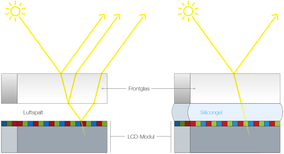
Bright light can make it much more difficult to read displays and touchscreens. This is the result of reflections and glare on the cover glass (left-hand graphic). Bonding with silicone gel (right) helps to suppress undesirable reflections. Optically bonded displays can be read without any difficulty outdoors.
In terms of the underlying physics, reflections can occur wherever a light wave abruptly encounters different propagation conditions. “This typically happens at the interface of two materials that have widely different refractive indices,” explains Dr. Müller. If the refractive index difference between the two materials is 0.1 or less, hardly any light is reflected and so virtually all of it enters the second material. The refractive index of air is 1.0. This is much smaller than that of the materials employed in LCDs, Their refractive index is usually between 1.4 and 1.5.
Nonetheless, with the right materials and an ingenious bonding technology, it is possible to suppress the reflections, as demonstrated by the industrial displays made by VIA optronics GmbH, an internationally successful display enhancement company. Based in Schwarzenbruck near Nuremberg, the company makes plug-in liquid crystal displays, e.g. for automotive diagnostic tools, for artificial horizons in aircraft and for central displays in vehicles. Daylight readability, ruggedness and reliability are the key specifications in these applications.
Two elements

Outgoing Inspection: displays and touch panels coming off the production line at VIA optronics GmbH are put through their paces before being shipped.
Modern liquid crystal displays essentially comprise two separate parts: the LCD module containing all the components for generating the screen content, and a second module mounted in front of it. The latter can be a touch panel, for example, like that found in a smartphone. However, as in the case of ultrabook computers, it could also just be a cover glass to protect the sensitive surface of the LCD module against external influences or to serve as a design element.
Between the cover unit and the LCD module is a small gap, This gap plays a key role in light propagation because air has a much lower refractive index than the adjacent materials. Consequently, ambient light striking the display is reflected at all three interfaces: the front face of the front module, its rear face, and the front face of the LCD module.
Each of these three faces reflects three to four percent of the ambient incident light. The potential of these planes to cause reflection in an individual case depends on the angle of incidence of the light and the precise values of the refractive indexes. The total of the three individual reflections is about 12 percent. Multiple reflections also occur. “When these are factored in as well, the figure can easily rise to nearer 20 percent,” warns Jürgen Eichner, founder and CEO of VIA optronics GmbH. And if the device has a touchscreen, the figure can be boosted to over 30 percent due to the metallization layer. There are several steps involved in making a display readable in daylight. First, choose the right components. “We only use cover glasses that have been given an anti-reflection coating,” stresses VIA optronics boss Eichner.
“Silicone gels came closest to meeting all of our requirements. So, we used them as a basis for formulating our bonding material.”
Jürgen Eichner, CEO, VIA optronicsSeries of measures

For test purposes, one half of this liquid crystal display was optically bonded with silicone gel. The non-bonded half on the left exhibits substantial reflection. The bonded half (right) is easy to read.
This surface treatment minimizes reflections which occur at the outermost of the three planes of reflection. Second, use only capacitive touch panels. These have a transparent conductive layer that is particularly thin and finely textured. They therefore reflect less light than other systems while transmitting a relatively large amount of the backlight. Internal planes of reflection are eliminated by bonding the LCD module and the module in front of it firmly to one another. Known as optical bonding, this measure is especially effective at reducing reflections. The reason is that the refractive index of the silicone adhesive roughly matches the refractive indexes of the two adjacent materials. As a result, the light can propagate as if the two joined parts and the adhesive were essentially all one material.
Together, the surface treatment and the optical bonding can reduce the reflectance to below one percent. In bright surroundings, the resultant display has a much higher contrast ratio than a standard display. “The final step is to optimize the backlighting, for example, by directing and bundling the light more effectively,” adds Eichner. This creates a more brilliant display and, because the eyes have adapted to the bright surroundings, they are better able to decipher the screen contents.
Flatter screens

For safety reasons, navigation device screens should always be easy to read: optical bonding makes this possible.
Optical bonding is a major step in the fight against undesirable reflections. It has been used since the 1980s to produce flat-screen displays in the armaments and aviation industries and eliminates roughly two-thirds of all reflections. It also protects the visible area inside the display unit against dust and moisture, makes the display more robust and supports flatter designs. VIA optronics, which has 15 years’ experience in the field of optical bonding, has been granted a patent for a process that utilizes a pourable silicone gel which it developed jointly with WACKER. The gel is applied as a liquid and gradually cures to a soft layer. The silicone is allowed to set until it no longer flows but is still tacky, and only then are the two display parts joined together.
“As the parts are being assembled, the silicone is already partly crosslinked but by no means fully cured,” explains silicone expert Philipp Müller. This dry, tacky state is important: if the silicone were still liquid during assembly, it could penetrate into the backlighting unit or even into the LCD cell. It needs to develop the necessary adhesion to the part surfaces. “The trick is to assemble the parts at just the right time,” stresses Müller. The first step in bonding is to create a layer of dry, tacky silicone on the rear face of the cover glass or the touchscreen. The thickness of the layer depends on the size of the display and the desired level of ruggedness, but is between 0.1 and 2 millimeters. And for vandal-proof displays, it may also be substantially greater. The parts are then brought together with no appreciable pressure to form a snug-fitting assembly. These steps are performed by VIA optronics in a cleanroom to prevent contamination of the bonding layer. The silicone adhesive then cures completely, and the bonded assembly attains its ultimate strength.
VIA optronics’ “dry process” requires extensive practical know-how and the right bonding material. “It will only work with the tailor-made silicone gel that WACKER makes exclusively for us,” says Jürgen Eichner from VIA optronics. His company experimented with many classes of transparent materials – not just silicones but also organic adhesives. However, the latter proved unsuitable because they had a tendency to turn yellow and shrink, among other things. “The search for the right material ultimately led us to WACKER. Its silicone gels came closest to meeting all of our requirements,” said Eichner. “So, we used them as a basis for formulating our bonding material.”
Soft and highly flexible:

Production of an optically bonded special display in the Mörsdorf development laboratory of VIA optronics GmbH.
Unlike conventional silicone rubbers, silicone gels do not vulcanize to a silicone elastomer. They yield a soft, highly flexible material that is closer to jello in consistency than rubber. In a crosslinked silicone gel, the individual polymer molecules are interconnected to form a loose, wide-mesh network. Some silicone chains are even connected by just one of their ends to the network. This network makes the cured rubber highly compliant and viscoelastic: the silicone gel can be deformed and takes time to return to its original shape. For WACKER application technologist Philipp Müller, this is important for use in displays: “The silicone gel can reliably cushion mechanical loads and mold snugly to solid surfaces.”
Silicone gels possess a further advantage: as addition-curing compounds, they undergo hardly any changes during curing. This property is essential for optical bonding, stresses VIA optronics CEO Eichner: “If the bonding layer were to shrink during curing, the edges of the bonded modules would come under tensile stress. That would impact the LCD cell and lead to visible color changes on the screen.”
“The silicone gel can reliably cushion mechanical loads and mold snugly to solid surfaces.”
Philipp Müller, Application Technology Industrial Solutions, WACKER SILICONESAbout VIA optronics
VIA optronics GmbH (www.via-optronics.com) is a globally active company in the field of display enhancement that specializes in the manufacture of low-reflection LCDs. The company has more than 16 years of experience and numerous patents in optical bonding. Displays developed or enhanced by VIA optronics are incorporated into devices that are designed especially for use outdoors or in brightly lit rooms, such as medical diagnostic devices, portable measuring instruments, navigation devices in cars and industrial robots. The company has 400 employees around the world and production sites in Mörsdorf, Germany, and Suzhou, China. It is headquartered in Schwarzenbruck near Nuremberg, Germany.
The silicone experts from WACKER joined forces with VIA optronics to devise a rough formulation for the silicone bonding material. This marked the beginning of a fruitful relationship. “It didn’t take us long to become convinced of the technological and commercial merits of using a silicone gel for optical bonding. That persuaded us to produce an exclusive product for VIA optronics,” says Müller.
As tablet computers and smartphones grow in popularity, consumers are becoming exceptionally fond of optically bonded touchscreens. The trend was started by Apple with its iPhones and iPads, which are operated via touchscreens. Microsoft is driving it further with its touchscreen-controlled Windows 8 operating system. “This has placed enormous pressure on makers of end-user devices to employ touchscreens,” estimates Prof. Blankenbach.
Optical bonding stands to benefit enormously from this trend in the years ahead. WACKER and VIA optronics recently agreed to work even more closely on optical bonding activities. The terms of the agreement provide for expert knowledge transfer in the development of new silicone products and processing technologies, and the bundling of distribution and marketing activities, so that glaring, hard-to-read displays will one day be a thing of the past.