
Silicon for the chip industry must meet what is known as the 12N purity standard – it must be 99.9999999999% pure, in other words.
Pure, Purer, WACKER Poly
WACKER POLYSILICON is the leading supplier of hyperpure polysilicon for semiconductor applications. Nearly half of all microchips worldwide are made with WACKER polysilicon. And with semiconductor manufacturers demanding increasingly pure material, WACKER is investing in the expansion and productivity of its polysilicon cleaning facility in Burghausen.
“Only the paranoid survive” was the title that Andy Grove, longtime CEO of Intel, gave to his memoir. The phrase expresses the demands for flawless products and ever-improving quality that define the microchip industry and that led to Moore’s law. Formulated by Intel co-founder Gordon Moore in 1965 based on observations of his industry, the law states that the number of transistors on a microchip doubles every one to two years, while structures become correspondingly smaller, and devices grow more powerful.
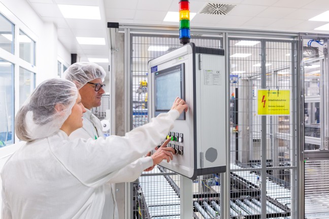
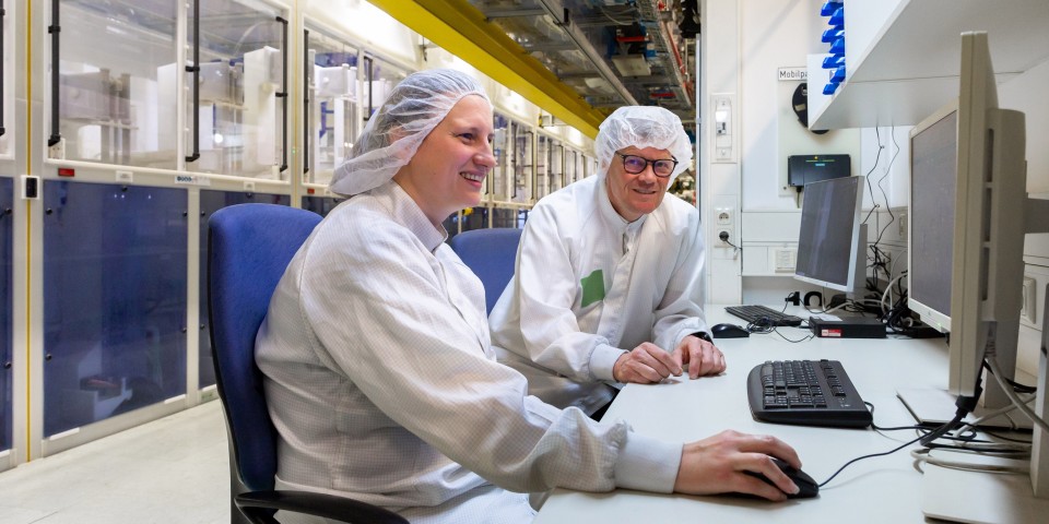
Michaela Waldhör (left) is the assistant shift leader in Poly Cleaning in Burghausen. Right: Armin Sandner, production manager for Semiconductor Poly.
Microchip performance has advanced considerably since that time. A current example is Apple’s A17 chip, which is featured in the latest iPhones. Based on highly advanced 3 nm technology, the chip contains 19 billion transistors and is capable of processing 35 billion operations per second. Modern chips like these deliver faster and faster processing speeds and enable applications like artificial intelligence and autonomous driving – applications that would have been dismissed as science fiction just a few decades ago. But they can do more than that: they also consume less energy, which helps protect the climate.
Chips like the A17 are the current manifestations of the development that Moore described nearly six decades ago. These kinds of performance enhancements are made possible by tremendous technology investments on the part of the semiconductor industry, which imposes its quality standards on the entire supply chain. Semiconductor manufacturers expect their suppliers to constantly optimize and develop their products and processes down to the tiniest detail until they have been perfected.
Increased performance requirements likewise have an impact on the starting material for most chips: hyperpure polycrystalline silicon. Neither the chip industry nor the solar industry could exist without this silicon. It must be purer than pure – critical foreign atoms are measured and specified in ppt (“parts per trillion” = one foreign atom to one trillion silicon atoms). Experts use the term 12N purity, which is defined as 99.9999999999% purity. To put all of this in more accessible terms, one ppt corresponds to a concentration of three sugar cubes in ten billion liters of water – the volume of one million tank trucks. And that purity must be guaranteed for every single bag in every delivery of polysilicon that we send to our customers.
Concentrations that small are beyond what we humans can imagine. WACKER POLYSILICON has an outstanding Analytical Services department, however, which can reliably detect even the tiniest traces of impurities – a truly unique selling point in the industry. And one of several reasons why WACKER POLYSILICON ranks as the world’s leading specialist for such high-purity silicon.
At its German sites in Burghausen and Nünchritz and its US site in Charleston, Tennessee, the company operates plants that manufacture this basic material. Michaela Waldhör is one of over 2,400 employees in this Wacker Chemie AG business division, where she works as assistant shift supervisor in the polysilicon cleaning facility in Burghausen. She finds the high quality standards fascinating: “We operate an elaborate infrastructure here so that we can meet the specifications of the chip industry. Achieving the quality they need means working together,” Waldhör explains. Around 60 team members currently work each shift. The plant runs non-stop, around the clock, seven days a week.
WACKER has almost 70 years of experience in polysilicon production, having begun producing this material for the emerging microelectronics industry as early as the mid-1950s. In WACKER POLYSILICON plants, metallurgical-grade silicon with a metalloid content of 98 to 99 percent is made into hyperpure silicon that meets the semiconductor industry’s 12N purity standard.
The metallurgical-grade silicon for this process comes from sources such as WACKER’s own production facility in Holla, Norway, and is then sent to the Burghausen, Nünchritz and Charleston sites for further processing. Here it is converted to liquid trichlorosilane, in which it is reacted with gaseous hydrogen chloride in a fluidized-bed reactor at 300 to 350 degrees Celsius. This trichlorosilane is then distilled to remove impurities. In the deposition reactor, the now extremely pure trichlorosilane is heated to over 1,000 degrees Celsius and passed over thin, U-shaped silicon rods using what is known as the Siemens process. The trichlorosilane then breaks down, depositing the silicon onto the surface of the rod, and the resulting hydrogen chloride is fed back into the process. At WACKER, this principle is called integrated production.
To produce the high-purity monocrystalline silicon wafers used as the precursors for chips, however, wafer manufacturers cannot use the polycrystalline material in this form. They need smaller chunks of silicon that melt more readily and can then be pulled to produce a perfect crystal. This is why the polysilicon rods are crushed.
However, the crushing tools in turn lead to (minor) contamination with foreign atoms. And every foreign atom impacts the required purity of the monocrystal and changes its physical properties. Phosphorus and boron in particular must be eliminated to the greatest possible extent. This is because some of these elements are later used for chip production in precisely defined trace concentrations in order to selectively modify the performance characteristics of the semiconductor components. But sodium, iron, carbon and other elements that occur naturally in combination with silicon must also be removed, as do elements that come into contact with the silicon during production, as they would severely affect the electrical properties of the chips.
Consequently, the surface of the polysilicon used in the semiconductor industry has to undergo a separate cleaning step after crushing. Its perfect mastery of these processes is one of WACKER POLYSILICON’s core competencies and a key reason for the division’s strong market position.
Her training as a master chemical technician gives Michaela Waldhör the expertise to do the job. Polysilicon cleaning involves both chemical and process-engineering steps.
- The first step is for employees to carry out a thorough visual inspection of the silicon chunks. Examples of sorting criteria include the size of the chunks and the quality of the surface, and any material that fails to meet critical requirements is culled.
- The inspected polysilicon chunks are then automatically transported in special trays to several immersion basins containing a precisely defined mixture of acids. This etches away a small amount of material, removing foreign atoms from the surface of the silicon chunks.
- In the next step of the processing sequence, the surface of the polysilicon is made hydrophilic and rinsed with ultrapure water.
- Finally, the silicon is dried before being packaged under clean room conditions.
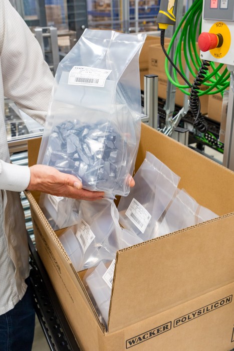
Semiconductor-grade polysilicon chunks are packaged under cleanroom conditions.
The entire process is precisely defined and qualified in detail with wafer manufacturers and the actual chip manufacturers. WACKER is currently expanding its polysilicon cleaning capacities in Burghausen. The topping-out ceremony will be held October 19. This additional capacity must meet the same technical requirements as existing plants, of course. In addition, the plant will also be equipped to meet the even higher purity requirements of the future.
In developing novel processes to achieve higher and higher degrees of purity, an in-house innovation group at WACKER worked with a carefully selected company specializing in mechanical and plant engineering. This is because the machinery and systems for each new process necessarily require innovative designs and specifications – otherwise there would be no way of running the new processes.
The business division is also continuing to develop its analytical processes, since even higher purity levels will have to be detected in the future. Future-proofing the overall process, in other words, means taking every single step into account.
The new plants will increase the existing capacity for cleaned polysilicon at the Burghausen site by well over 50 percent. The business division is investing more than 300 million euros in the new cleaning line, which is scheduled to go on stream at the beginning of 2025. The project, which is part of the EU’s “Important Projects of Common European Interest” (IPCEI) program, will receive financial support in the amount of 46 million euros from the Federal Ministry for Economic Affairs and Climate Protection, the EU and the State of Bavaria.
“Hyperpure polysilicon from WACKER is an indispensable raw material for the global economy. Megatrends like digitalization, artificial intelligence and electromobility are driving demand for it,” explains Dr. Tobias Brandis, president of WACKER POLYSILICON. “Our new cleaning line in Burghausen gives us the foundation we need to continue meeting the rapidly growing demand of our semiconductor customers. Thanks to this investment, we will also be able to take the quality of our material to the next level and extend our support to the semiconductor sector’s latest technologies.”
The industry is of enormous economic importance for Germany and Europe – not least because semiconductors are critical for the digital and green transformations of the economy. As a result, the EU has set itself a goal of establishing 20 percent of the world’s microelectronics production in Europe by 2030. “We’re proud to be one of a total of 56 companies that are part of the IPCEI cluster,” Dr. Brandis emphasizes. “As Europe’s only producer of hyperpure polysilicon for semiconductor applications, our etching line project will play an important role in strengthening Europe’s chip production supply chain over the long term.”


The business division has channeled decades of expertise into building the new cleaning line in Burghausen: “We have to master the process engineering, chemistry and mechanical engineering ourselves – you can’t just buy some off-the-rack plant to get the purity our customers need,” points out Armin Sandner, head of Semiconductor Poly at WACKER.
And this also applies to the team members. As sophisticated and automated as WACKER POLYSILICON’s processes are, product quality ultimately still depends on experienced and dedicated employees. By expanding its polysilicon cleaning capacities, WACKER is creating more than 100 new, attractive jobs in Burghausen. The Charleston site will benefit from the expansion too, as the project will allow the company to take hyperpure polysilicon made in the US and upgrade it in Germany – and that, in turn, will help us continue strengthening connections and collaboration across the Atlantic.
The enormous significance of semiconductor-grade silicon never fails to impress and excite Michaela Waldhör, the assistant shift leader from Poly Cleaning in Burghausen. “Every single day, each and every one of us inevitably uses technology that you couldn’t have without our silicon,” she says.
Even if the WACKER brand name does not appear on the end products, the company’s expertise is what keeps our smartphones, computers and the internet – our day-to-day lives, in other words – up and running.