
Our system has noticed that you are based in , but the current country setting is . Select country

Polysilicon
From silicon to value
Hyperpure polysilicon is the bedrock of modern microelectronics, and we lead the world in its production.
As a quality and technology leader, we deliver polysilicon that meets the purity and reliability standards that semiconductor makers need in order to manufacture high-performance microchips.
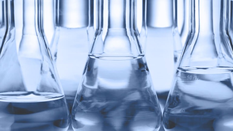
Polysilicon for the semiconductor and solar industries
The digital age is here to stay. Notebooks, cell phones, cars, washing machines, you name it – in today’s world, nothing works without microprocessors and memory chips. Most semiconductor chips are based on polycrystalline silicon, a material also known as polysilicon and, in everyday speech, often referred to as just “silicon.” Without polysilicon – which is what lends semiconductors their critical properties – neither the chip industry nor the solar industry would exist.
A pioneer in silicon, we began producing polysilicon on an industrial scale in 1959 and have been growing our expertise in photovoltaics since the early 2000s. Today, we are one of the world’s leading suppliers of this crucial raw material for microelectronics and solar energy.
Supporting the development of digital technology for over 70 years
WACKER’s new cleaning line in Burghausen comes on stream, producing hyperpure silicon for the digital age and setting new standards in silicon purity.

WACKER invests $2.5 billion and opens a new production site for hyperpure silicon in Charleston, USA. In Burghausen, Germany, WACKER invests in a new cleaning line – keeping pace with the semiconductor industry.

Since 2005, WACKER has invested over €2 billion in the expansion of its sites in Nünchritz and Burghausen, Germany.

Focusing on expanding its capacities and capabilities for hyperpure silicon, WACKER builds the first industrial-scale cleaning plant in the 1990s, timed to coincide with the introduction of 200 mm silicon wafers.

WACKER becomes the leading producer of semiconductor-grade silicon. Our long-term standing in the market is underpinned by over 50 years of unwavering commitment to quality and reliability.

WACKER begins industrial-scale production of silicon for semiconductors. Texas Instruments and Fairchild develop the first integrated circuit (IC) – a groundbreaking invention and the basis of Moore's Law.

WACKER starts systematic research and development on hyperpure silicon for the semiconductor industry.

Hyperpure polysilicon for the digital age

View of the Etching Line Next production facility. Acids are used for cleaning the polysilicon chunks before they are shipped to semiconductor customers throughout the world.
Etching Line Next
A state-of-the-art production line for cleaning the surface of semiconductor-grade polysilicon has begun operations at WACKER’s Burghausen site. This new etching line has boosted cleaning capacity by more than 50% and further increased the surface purity of the polysilicon – a decisive factor in shaping current and future generations of semiconductors. The fully automated process uses special acid etching techniques and cleanroom technology to meet the most exacting microelectronics requirements.
Every new generation of digital devices tends to operate at higher and higher switching frequencies, which is how they become faster and more powerful. This progress is made possible through advances in miniaturization of the physical features created inside the chips. Increasing performance demands imposed on chips also have an impact on the raw material, which means that the polysilicon used must be extremely pure. Why? Because foreign atoms in the silicon would change the electrical properties of the semiconductor and could cause chips to fail. Hyperpure polysilicon ensures that the tiny transistors inside modern chips work reliably and predictably, which also helps chips last longer – after all, impurities can shorten chip life. Hyperpure material helps keep chips working reliably for many years.


From silicon to value
The production of polysilicon begins with the raw material: sand. The primary component of sand is silicon dioxide, from which metallurgical-grade silicon is extracted to a purity level of 98 to 99 percent.
However, the purity and quality requirements of the electronics and photovoltaic industries are extraordinarily high – as a result, more highly specialized steps are needed in order to produce polysilicon. The illustrations below provide more information on this process.
An important aspect of the manufacturing process, especially of the Siemens process, is its exceptionally high energy demand – a huge amount of electricity is needed. WACKER has long been a pioneer here, having extensively electrified our processes and invested consistently in renewable energies. Doing so has resulted in an especially low CO2 footprint and consequently played a major role in creating a sustainable value chain.
Our hyperpure silicon is sliced into thin wafers. These wafers serve as the basis for producing the electronic chips that will be used in future microelectronics applications, such as AI computing centers or the 5G technologies that will continue linking our digital world together.
We have carefully optimized our cleaning process with an eye to effectively eliminating foreign atoms, greatly expanding the range of applications for our polysilicon – such as highly sensitive communications technology or camera chips in smartphones. Hyperpure silicon, in other words, is essential to the next generation of chips. Our process is ITAF-certified and reflects decades of experience in this industry.
The key stages in hyperpure polysilicon production
1. Quartz
Silicon is the second most abundant element on earth. In nature, it primarily exists as silicon dioxide (SiO2), most commonly found in the form of quartz.

2. Metallurgical-grade silicon
Heating silicon dioxide (SiO2) with carbon removes the oxygen atoms to generate metallurgical-grade silicon (Simg) at a purity level of roughly 98 to 99% – not high enough for the semiconductor or photovoltaic industries. To boost the purity, WACKER uses a tried-and-tested distillation process.

3. Fluidized-bed reactor
The first step is to react metallurgical-grade silicon (Simg) with hydrogen chloride (HCl) in a fluidized-bed reactor. This converts it to liquid trichlorosilane (HSiCl3).
Simg + 3 HCl -> SiHCl3 + H2

4. Trichlorosilane distillation
This liquid is then distilled to remove the impurities and generate extremely pure trichlorosilane.

5. Silicon deposition reactor
The next step is the energy-intensive process of heating the trichlorosilane distillate to approximately 1,000 °C and passing it over thin, heated silicon rods.

6. Pure silicon
The trichlorosilane breaks down during this process, allowing pure silicon to deposit on the surface of the rods.
4 SiHCl3 -> Si + 3 SiCl4+ 2 H2

7. Silicon chunks
Next, we chop the hyperpure silicon into smaller pieces. The resulting chunks are the starting material for solar cells and semiconductor wafers. In order to use chips in the microelectronics applications of the future, yet another step is needed: cleaning the surface of the silicon. This exceptionally thorough process involves removing undesired trace materials and impurities, with the aim of eliminating virtually all foreign atoms from the material and its surface.

Worldwide production sites
We draw on our 70 years of experience to produce hyperpure polysilicon for the semiconductor and photovoltaic industries at the following three sites:


