Leading Positions In Semiconductors And High-Performance Solar Cells
Nearly Half Of All Computer Microchips Contain WACKER Polysilicon
Polysilicon for the Semiconductor and Solar Industries
The digital age is here to stay. Notebooks, cell phones, cars, washing machines, you name it – in today’s world, nothing works without microprocessors and memory chips. Most semiconductor chips are based on silicon. Polysilicon too is often called silicon. It is the material that possesses the semiconductor properties and, without it, there would be no chip industry and no photovoltaics industry.
A pioneer in the industry, we have been producing polysilicon on an industrial scale since 1959. From the early 2000s, we have increasingly extended our expertise to photovoltaics as well. Today, we are one of the world's leading suppliers of this key raw material for microelectronics and solar energy.
PART OF DIGITAL DEVELOPMENTS FOR MORE THAN 70 YEARS
Etching Line Next
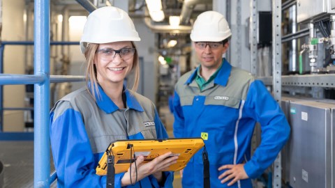
View of the Etching Line Next production facility. Acids are used to clean the polysilicon chunks before they are ready to be shipped to semiconductor customers across the world.
Hyperpure Polysilicon for the Digital Age
WACKER has commissioned a state-of-the-art etching line for surface cleaning of semiconductor-grade polysilicon at its Burghausen site. This new line has boosted cleaning capacity by more than 50 % and further increased the surface purity of the polysilicon – a decisive factor in the shaping of current and future semiconductor generations. The fully automated process uses special acid etching techniques and cleanroom technology to meet the most exacting microelectronics requirements.
Every new generation of digital devices tends to operate at higher switching frequencies. That is how they become faster and more powerful. This progress is made possible through advances in the miniaturization of the physical features generated inside the chips. The ever-increasing performance demands imposed on chips also have an impact on the raw material. It is therefore indisputable that the polysilicon used must be extremely pure. Why? Because foreign atoms in the silicon would alter the electrical properties of the semiconductor and could lead to chip failure. Hyperpure polysilicon safeguards the stability and performance of the tiny transistors inside modern chips, ensuring they operate reliably and predictably while also contributing to chip longevity: because foreign-atom impurities shorten chip life. Hyperpure material helps to ensure that the chips perform reliably for many years.
From Silicon to Value
The production of polysilicon begins with the raw material: sand. Sand is mainly composed of silicon dioxide, and the first step is to extract metallurgical-grade silicon from it with a purity of around 98 to 99 percent.
However, the purity and quality requirements are so high that further steps are needed to produce polysilicon that is suitable for the electronics and photovoltaic industries. More information on this is provided in the schematic diagram below.
An important aspect of the manufacturing process, especially the Siemens process, is its exceptionally high energy demand. It requires a vast amount of electricity to run. But WACKER, ever the pioneer, has electrified its processes with renewable energy. As a result, its carbon footprint is particularly small – supporting a more sustainable value chain.
Our hyperpure silicon is sliced into thin wafers. These form the basis for the production of electronic chips for future microelectronic applications, such as 5G, and the further build-out of the world’s digital networks and AI data centers. Our cleaning process is also carefully optimized to remove foreign atoms. This extends the usability of polysilicon for communications technologies and smartphone camera chips. Hyperpure silicon is therefore essential to the next chip generation.
Our process is ITAF-certified and reflects decades of experience in this industry.
The Key Stages In The Production Of Hyperpure Polysilicon:
Worldwide Production Sites
We draw on our 70 years of experience to produce hyperpure polysilicon for the semiconductor and photovoltaic industries at the following three sites.
Burghausen (Germany)Charleston, Tennessee (USA)
Nünchritz (Germany)


